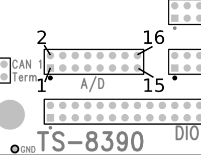
TS-8390-47xx ADC Header
The Analog to Digital Converter consists of a 4-channel 16 bit sigma-delta converter and two, 2-channel analog switches. These are configured to allow input and conversion on two differential channels and 4 single ended channels. The 6-channel Analog to Digital signals are contained on connector HD5 which is a 16 pin (2x8) 0.1" spacing header. The connector layout and the signals carried by each pin are defined below. The input range for the differential input channels is 0- 2 VDC, and the input range on the single-ended channel is nominally 0-10 VDC.
Our default core shipped with the TS-4710 does not include support for ADC. Support can be included with this opencore bitstream. See the FPGA section for more information on loading this bitstream, or building a custom one.
This example prints out all 6 ADC readings in millivolts:
#include <stdio.h>
#include <stdint.h>
#include <sys/mman.h>
#include <sys/stat.h>
#include <assert.h>
#include <fcntl.h>


volatile uint16_t *syscon = 0;
inline void syscon_init() {
	if(syscon == 0) {
		int mem = open("/dev/mem", O_RDWR|O_SYNC);
		syscon = mmap(0,
			getpagesize(),
			PROT_READ|PROT_WRITE,
			MAP_SHARED,
			mem,
			0x80004000);
	}
}

uint16_t peek16(uint16_t addr)
{
	syscon_init();
	return syscon[addr/2];
}

void poke16(uint16_t addr, uint16_t value)
{
	syscon_init();
	syscon[addr/2] = value;
}

int main()
{
	int x, i;

	// Select AN_SEL line:
	// For the TS-TPC-8390 baseboard:
	poke16(0x400, 0x28);

	// enable all 6 channels
	poke16(0x402, 0x3f);

	// allow time for conversions
	usleep(500000);

	for (i = 1; i <= 6; i++) {
		x = (signed short)peek16(0x402 + 2*i);
                if (i > 2) x = (x * 1006)/200;
                x = (x * 2048)/0x8000;
                printf("adc%d=%d\n", i, x);
	}

	return 0;
}
Running this code on the TS-TPC-8390 with pin 7 of the ADC header (channel 3) connected to 3.3V returns:
 root@ts4700:~# ./adctest
 adc1=0
 adc2=0
 adc3=3302
 adc4=0
 adc5=0
 adc6=0
| Offset | Bits | Description | |||||||||
|---|---|---|---|---|---|---|---|---|---|---|---|
| 0x0 | 15:8 | Core ID register (reads 0xad) | |||||||||
| 7:6 | Reserved | ||||||||||
| 5:4 |
| ||||||||||
| 3:2 |
| ||||||||||
| 1:0 |
| ||||||||||
| 0x2 | 15:0 | Channel Mask | |||||||||
| 0x4 | 15:0 | Channel 1 most recent conversion value | |||||||||
| 0x6 | 15:0 | Channel 2 most recent conversion value | |||||||||
| 0x8 | 15:0 | Channel 3 most recent conversion value | |||||||||
| 0xa | 15:0 | Channel 4 most recent conversion value | |||||||||
| 0xc | 15:0 | Channel 5 most recent conversion value | |||||||||
| 0xe | 15:0 | Channel 6 most recent conversion value |
The channel mask register controls which channels are enabled. Bits 0-5 enable channels 1-6 respectively. If a given channel is not enabled, (enable bit == 0) it will not be sampled and its conversion value register will contain an obsolete and meaningless value. The more channels that are enabled, the lower the sampling speed on each channel.
