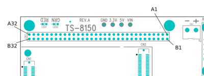
The PC/104 connector consists of two rows of pins labeled A and B, the numbering of which is shown below. The signals for the PC/104 interface are generated by a MAX240 PLD on the TS-8150. It converts the MUXBUS cycles from the SoM to PC/104 bus cycles and provides some GPIO pins for finer control of the PC/104 interface.
Any of the I/O labeled DIO_* can be controlled through manipulation of the TS-8150 registers directly. See the PC/104 interface section for more information on how the pins are driven.
| Pin
|
Name
|
Pin
|
Name
|
| A1
|
BUS_BHE#
|
B1
|
Ground
|
| A2
|
ISA_D_07
|
B2
|
ISA_RESET
|
| A3
|
ISA_D_06
|
B3
|
5 V
|
| A4
|
ISA_D_05
|
B4
|
AD_08
|
| A5
|
ISA_D_04
|
B5
|
3.3 V out
|
| A6
|
ISA_D_03
|
B6
|
Not connected
|
| A7
|
ISA_D_02
|
B7
|
Not connected
|
| A8
|
ISA_D_01
|
B8
|
Not connected
|
| A9
|
ISA_D_D0
|
B9
|
VIN
|
| A10
|
ISA_WAIT#
|
B10
|
Ground
|
| A11
|
ISA_ADD_20
|
B11
|
DIO_B11
|
| A12
|
ISA_ADD_19
|
B12
|
DIO_B12
|
| A13
|
ISA_ADD_18
|
B13
|
ISA_IOW#
|
| A14
|
ISA_ADD_17
|
B14
|
ISA_IOR#
|
| A15
|
ISA_ADD_16
|
B15
|
Not connected
|
| A16
|
ISA_ADD_15
|
B16
|
Not connected
|
| A17
|
ISA_ADD_14
|
B17
|
ISA_D_09
|
| A18
|
ISA_ADD_13
|
B18
|
ISA_D_10
|
| A19
|
ISA_ADD_12
|
B19
|
DIO_B19
|
| A20
|
ISA_ADD_11
|
B20
|
ISA_D_12
|
| A21
|
ISA_ADD_10
|
B21
|
ISA_IRQ7
|
| A22
|
ISA_ADD_09
|
B22
|
ISA_IRQ6
|
| A23
|
ISA_ADD_08
|
B23
|
ISA_IRQ5
|
| A24
|
ISA_ADD_07
|
B24
|
Ground
|
| A25
|
ISA_ADD_06
|
B25
|
ISA_D_11
|
| A26
|
ISA_ADD_05
|
B26
|
ISA_D_13
|
| A27
|
ISA_ADD_04
|
B27
|
ISA_D_14
|
| A28
|
ISA_ADD_03
|
B28
|
ISA_D_15
|
| A29
|
ISA_ADD_02
|
B29
|
5 V
|
| A30
|
ISA_ADD_01
|
B30
|
ISA 14.3 MHz
|
| A31
|
ISA_ADD_00
|
B31
|
Ground
|
| A32
|
Ground
|
B32
|
Ground
|
|
|
| WARNING:
|
Most of the pins on the PC104 bus are 3.3 V tolerant. Refer to the schematic for more details.
|
