TS-7400 V2 DIO
This board uses CPU DIO, typically there are 4 functions associated with each physical pin (I2C, PWM, SPI, DIO, etc). See the CPU manual for the complete listing and for information on how to control these DIO.
Note that most of the pins start in their "Function" mode and must be set to DIO mode to be able to be used as DIO. Be aware that doing this on a running system may have adverse effects if there are kernel drivers trying to use specific pins in their peripheral mode(s).
DIO numbers are referenced in <bank>_<pin> notation in the table below. This makes associating pins with DIO registers much simpler when looking at the manual. The example code below is also based around using the bank and pin notation.
DIO can be directly manipulated with tshwctl, for example:
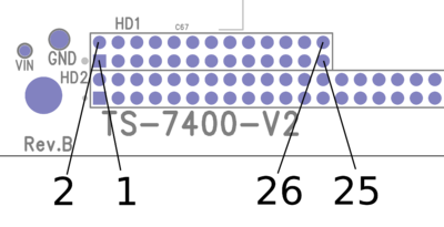
tshwctl --setdio 3_25 #Set pin 1 of the 26 pin header high
tshwctl --clrdio 0_17 #Turn on the red LED by setting the pin low
tshwctl --getdio 1_16,1_17 #Get the input state of pin 1 and 3 of the 44 pin header
See the end of this section for example software to manipulate DIO pins.
Upper header pin-out (26-pin)
|

|
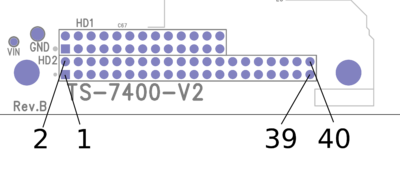
Lower header pin-put (40-pin)
|

|
Other
| Name | DIO |
|---|---|
| GRN_LED# | CPU DIO0_28 |
| RED_LED# | CPU DIO0_17 |
| EN_ETH_POWER# | CPU DIO0_6 |
| EN_USB_5V | CPU DIO1_27 |
| EN_CAN# | CPU DIO3_30 |
Example code for CPU DIO manipulation:
#include <assert.h>
#include <fcntl.h>
#include <string.h>
#include <stdio.h>
#include <stdlib.h>
#include <sys/mman.h>
#include <sys/stat.h>
#include <sys/types.h>
#include <unistd.h>

#define DIO_Z 2
volatile unsigned int *pinctl = NULL;

/*******************************************************************************
* setdiopin: accepts a DIO register and value to place in that DIO pin.
*   Values can be 0 (low), 1 (high), or 2 (z - high impedance).
*******************************************************************************/
void setdiopin(int bank, int pin, int val)
{
	if(val == 2) {
		pinctl[((0xB00) + (0x10 * bank) + 0x8)/4] = (0x1 << pin);
	} else {
		pinctl[((0x700) + (0x10 * bank) + (0x8 / (val+1)))/4] =
		  (0x1 << pin);
		pinctl[((0xB00) + (0x10 * bank) + 0x4)/4] = (0x1 << pin);
	}
}
/*******************************************************************************
* getdiopin: accepts a DIO pin number and returns its value.
*******************************************************************************/
int getdiopin(int bank, int pin)
{
	return (((pinctl[((0x900) + (0x10 * bank))/4]) >> pin) & 0x1);
}

/*******************************************************************************
* Main: accept input from the command line and act accordingly.
*******************************************************************************/
int main(int argc, char **argv)
{
	int devmem = 0;
	int pin, bank, reg = 0, muxpin;
	int val;
	int returnedValue;

	// Check for invalid command line arguments
	if ((argc > 4) | (argc < 3)) {
		printf("Usage: %s bank pin [0|1|2]>\n", argv[0]);
		return 1;
	}

	// We only want to get val if there are more than 3 command line arguments
	if (argc == 3) {
		bank = strtoul(argv[1], NULL, 0);
		pin = strtoul(argv[2], NULL, 0);
		val = 0;
	}
	else {
		bank = strtoul(argv[1], NULL, 0);
		pin = strtoul(argv[2], NULL, 0);
		val = strtoul(argv[3], NULL, 0);
	}

	assert(bank >= 0 && bank < 5);
	assert(pin >= 0 && pin < 32);
	assert(val >=0 && val < 3);

	devmem = open("/dev/mem", O_RDWR|O_SYNC);
	pinctl = mmap(0, getpagesize(), PROT_READ|PROT_WRITE, MAP_SHARED, devmem, 0x80018000);

	/* We determine what muxsel reg we need, and set the right pin to DIO*/
	if(pin > 15) {
		reg = 1;
		muxpin = pin - 16;
	} else muxpin = pin;
	pinctl[((0x100) + (0x20 * bank) + (0x10 * reg) + 0x4)/4] = (0x3 << (muxpin * 2));

	// Parse through the command line arguments, check for valid inputs, and exec
	if (argc == 3) {
		returnedValue = getdiopin(bank, pin);
		printf("dio_%d_%d=%d\n", bank, pin, returnedValue);
	} else if(argc == 4) {
		setdiopin(bank, pin, val);
	}
	return 0;
}