TS-1420
 | |||
| Released May. 2014 | |||
| Documentation | |||
|---|---|---|---|
| FTP Path | |||
| DOUT | |||
| 12 | |||
| External Interfaces | |||
| 2x RJ45 Modbus / USB / 6x 4 Pin IO | |||
| Power Requirements | |||
| 8-28V Modbus | |||
| 5V USB | |||
| Operates around ?? | |||
| Operating Temperature | |||
| |||
| |||
| Mechanical | |||
| 140mm x 102mm | |||
Overview
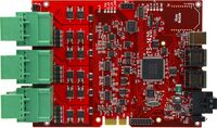
The TS-1420 is a Modbus peripheral providing 12 PWM capable FET output switches, rated at 8 Amps each, from an 8-30 VDC external supply, and 18 ADC channels connected internally to the FET channels to provide current in mA and voltage in mV on a per channel basis, to monitor power use on each channel.
Getting Started
Power Requirements
The TS-1420 will operate within a range of 10-28 VDC on either Modbus port. Power supplied on the Modbus port is passed along the bus as an active power rail on the other Modbus port. Do not apply power to both Modbus ports.
Features
TS Modbus Support
The TS-1420 can be utilized as a device in a chain of devices on the RS-485 Modbus port; or, as a single peripheral device on a USB port. When operating on the USB port, the default device address is 0xf6 (246) and the default bit rate is 1,000,000 bps.
When using all Technologic Systems Modbus devices we include functionality to create an arbitrary chain of stock peripherals to automatically enumerate all connected devices, configure them, and generate an I/O map of all connected devices.
TS Modbus Autoconfiguration
The autoconfiguration works by using the optional mode pin on the RJ45 connector as designated in the MODBUS-2W standard. Technologic Systems uses this to indicate if it is a TS device. If it is asserted (low) to a TS device, then it will allow access to the #Holding Registers at address 0xf7.
This will identify the TS Modbus device model, set the first device in the chain to the user specified slave address (default is 0x10), and assert the mode line to the next port to enumerate the next device. The next device address is incremented by 1, and the process is repeated until no slave responds to a read query (timeout)indicats that no additional devices are connected to the bus chain. At this point the last device in the chain is configured to enable bus termination on the RS485 link, and all devices have their bit rates set to the user selected bit rate (default is 9600).
Funciontality
The TS-1420 provides the following electrically (optically) isolated interfaces:
- 12 digital outputs with 6-bit PWM each driving s FET with 8 Amp sink capacity
- 12 Single Ended ADC channels directly connected to FET channels 0-11 constantly mesauring current in mA.
- 6 Single Ended ADC channels directly connected to FET channel pairs 0:1, 2:3, 4:5, 6:7, 8:9, 10:11 constantly measuring voltage in mV.
The ADC channels can be be set as a block for resolution (and associated sample rate) as follows:
- 12 bits per sample @ 240 SPS
- 14 bits per sample @ 60 SPS
- 16 bits per sample @ 15 SPS
Register Interface
Holding Registers
The interface to all Modbus peripheral devices consists of a set of 127 holding registers. These registers are used to configure the device operation, read and write input output parameters, as well as various settings used to configurable Modbus Address, Termination enable, Data Format, and Bit Rate. These settings are common to all of our Modbus peripherals and can be persisted in on-board flash memory.
NOTE: The device operates ONLY in Modbus RTU communications mode. Modbus ASCII is not presently supported.
| Address (hex) | Address (dec) | Access | Description | Example Values |
|---|---|---|---|---|
| 0x70 | 112 | Read/Write | Modbus Mode | 0 = ASCII (unimplemented), 1 = RTU |
| 0x71 | 113 | Read/Write | RS485 Bus Termination Enable | 0 = Termination disabled, 1 = Termination enabled |
| 0x72 | 114 | Read/Write | Modbus Device Address | 0-247 (0x00-0xf7) 0 = Broadcast |
| 0x73 | 115 | Read/Write | Modbus bit rate | Bit Rate |
| 0x74 | 116 | Read Only | Unit Model | e.g., 0x1400, 0x1700, 0x1800, etc |
| 0x75 | 117 | Read Only | Verilog Version | e.g., 1 |
| 0x76 | 118 | Read Only | ZPU Version | e.g., 1 |
| 0x77 | 119 | Read Only | Bus power Supply in millivolts | e.g., 23600 |
| 0x78 | 120 | Read Only | Internal Temperature in 1/100th degree Celsius | e.g., 290 |
| 0x79 | 121 | Read/Write | Reserved or model specific | Not applicable or model specific |
| 0x7a | 122 | Read/Write | Reserved or model specific | Not applicable or model specific |
| 0x7b | 123 | Read/Write | Reserved or model specific | Not applicable or model specific |
| 0x7c | 124 | Read/Write | Reserved or model specific | Not applicable or model specific |
| 0x7d | 125 | Read/Write | Write listed value to persist communications (Bit rate, Data format, Address, and Termination) parameters to internal nonvolatile storage: | 0xFEED = Persist configuration, 0xDEAD = Erase configuration, 0xC0DE apply configuration without persistence. In all cases the value is set to zero when completed or 0xFA17 (FAIL) if error. |
| 0x7e | 126 | Read/Write | Reserved or model specific | Not applicable or model specific |
NOTE: All Read Only registers may be written; however, writing to certain registers (e.g., Unit Model) will overwrite the information that will not be refreshed until the unit is reset.
Operational (holding) Registers
| Address (hex) | Address (dec) | Access
e Description | |
|---|---|---|---|
| 0 | 0 | Read / Write | Channel 0 ADC Result (FET current in mA) |
| 1 | 1 | Read / Write | Channel 1 Result (FET current in mA) |
| 2 | 2 | Read / Write | Channel 2 Result (FET current in mA) |
| 3 | 3 | Read / Write | Channel 3 Result (FET current in mA) |
| 4 | 4 | Read / Write | Channel 4 Result (FET current in mA) |
| 5 | 5 | Read / Write | Channel 5 Result (FET current in mA) |
| 6 | 6 | Read / Write | Channel 6 Result (FET current in mA) |
| 7 | 7 | Read / Write | Channel 7 Result (FET current in mA) |
| 8 | 8 | Read / Write | Channel 8 Result (FET current in mA) |
| 9 | 9 | Read / Write | Channel 9 Result (FET current in mA) |
| A | 10 | Read / Write | Channel 10 Result (FET current in mA) |
| B | 11 | Read / Write | Channel 11 Result (FET current in mA) |
| C | 12 | Read / Write | Channels 0:1 Result (FET pair voltage in mV) |
| D | 13 | Read / Write | Channels 2:3 Result (FET pair voltage in mV) |
| E | 14 | Read / Write | Channels 4:5 Result (FET pair voltage in mV) |
| F | 15 | Read / Write | Channels 6:7 Result (FET pair voltage in mV) |
| 10 | 16 | Read / Write | Channels 8:9 Result (FET pair voltage in mV) |
| 11 | 17 | Read / Write | Channels 10:11 Result (FET pair voltage in mV) |
| 12 | 18 | Read / Write | FET 0 Control |
| 13 | 19 | Read / Write | FET 1 Control |
| 14 | 20 | Read / Write | FET 2 Control |
| 15 | 21 | Read / Write | FET 3 Control |
| 16 | 22 | Read / Write | FET 4 Control |
| 17 | 23 | Read / Write | FET 5 Control |
| 18 | 24 | Read / Write | FET 6 Control |
| 19 | 25 | Read / Write | FET 7 Control |
| 1A | 26 | Read / Write | FET 8 Control |
| 1B | 27 | Read / Write | FET 9 Control |
| 1C | 28 | Read / Write | FET 10 Control |
| 1D | 29 | Read / Write | FET 11 Control |
| 22 | 34 | Read / Write | DIO OUTPUT: Bits 0-11 are reflected to the corresponding DIO output pins subject to the control of the associated DIO control registers (0x12-0x1D) |
| 0x40-0x4F | 64-79 | Read / Write | Reserved: Warning: Do not access location 64 (0x40) of DIO operations can become spurious |
| 60 | 96 | Read / Write | ADC Channel Resolution & Speed (One setting for all channels) |
| 65 | 101 | Read Only | High serial number (MAC) |
| 66 | 102 | Read Only | Middle serial number (MAC) |
| 67 | 103 | Read Only | Low serial number (MAC) |
Output Channel Control Register
| Bit 15 | Bits 14-6 | Bits 5-0 |
|---|---|---|
| 1: Direct DIO output; 0: PWM DIO output | Unused (Reserved) | PWM Value - 0: Off; 63: 98.4% On |
NOTE: Registers marked as Read Only may actually be written; however, the contents will not be refresehd until the unit is reset, and writing these registers will have no effect on the unit operation.
The PWM is scaled in increments of 1/64 (1.56%) per bit in the range of 0/64 through 63/64. To set 100% you must set the Direct DIO Output bit in this register and then set the appropriate bit in the direct output register at holding register 34 (hex 22). NOTE: The PWM range is 0 to 98.4%. The easiest way to do direct per bit control is the set the appropriate output control register (0x12-0x1D) to 0x8000 and manupulate the bit in DIO Output (0x22). To use the full range of the PWM, set the appropriate output register bit (0x22) to 1. Then set the ADC control register to a value from 0 to 63 (0-98.4%) or 0x8000 (100%).
ADC Channel Resolution & Speed Register Details
- Resolution and Speed
- 0: 11 bits @ 240 sps
- 1: 14 bits @ 60 sps
- 2: 16 bits @ 15 sps)
ADC Channel Resolution (and implied speed) values
| Value | Resolution (Bits) | Speed (Samples per Second) |
|---|---|---|
| 0 | 12 | 240 |
| 1 | 14 | 60 |
| 2 | 16 | 15 |
Communications Bit Rates
The TS-1420 supports 15 speeds:
| Value | Communication Bit Rate | Maximum CAT5 Cable Length |
|---|---|---|
| 0 | 300 | 1200 meters |
| 1 | 600 | 1200 meters |
| 2 | 1200 | 1200 meters |
| 3 | 2400 | 1200 meters |
| 4 | 4800 | 1200 meters |
| 5 | 9600 | 1200 meters |
| 6 | 19.2K | 1200 meters |
| 7 | 38.4K | 1200 meters |
| 8 | 57.6K | 1200 meters |
| 9 | 115.2K | 800 meters |
| 10 | 230.4K [1] | 400 meters |
| 11 | 460.8K [1] | 200 meters |
| 12 | 1040K [1] | 100 meters |
| 13 | 2080K [1] | 40 meters |
| 14 | 4160K [1] | 20 meters |
Connectors
Bus and Power connecttors
From left: LED Status indicators, External power (8-28 VDC), 2X Modbus RJ-45, USB
Both RJ45 ports, and all of our Modbus based devices are designed to be compatible with 2W-MODBUS RJ-45 following this pinout:
| Pin | Signal |
|---|---|
| 1 | Ground |
| 2 | Ground |
| 3 | Mode |
| 4 | Data (+) |
| 5 | Data (-) |
| 6 | 12-24 VDC |
| 7 | 12-24 VDC |
| 8 | Ground |
24 Pin Removable Terminal Blocks
The two terminal blocks contain 3 removable 4x2 pin connectors (P3 / P4 / P5) that provide all of the FET digital output connections as listed below.
P3/4/5/A / P3/4/5/B - Top & Bottom Connector Signal Layout
| Top | Left (P3-A) | Middle (P4-A) | Right (P5-A) |
|---|---|---|---|
| Bottom | Left (P3-B) | Middle (P4-B) | Right (P5-B) |
| Connector | Pin 1 Signal Description | Pin 2 Signal Description | Pin 3 Signal Description | Pin 4 Signal Description |
|---|---|---|---|---|
| P3-A (Top Left) | V+ Channel 4 & 5 | FET Switch 4 | FET Switch 5 | Isloated Gounrd |
| P3-B (Bottom Left) | V+ Channel 6 & 7 | FET Switch 6 | FET Switch 7 | Isloated Gounrd |
| P4-A (Top Middle) | V+ Channel 8 & 9 | FET Switch 8 | FET Switch 9 | Isloated Gounrd |
| P4-B (Bottom Middle) | V+ Channel 10 & 11 | FET Switch 10 | FET Switch 11 | Isloated Gounrd |
| P5-A (Top Right) | V+ Channel 0 & 1 | FET Switch 0 | FET Switch 1 | Isloated Gounrd |
| P5-B (Bottom Right) | V+ Channel 2 & 3 | FET Switch 2 | FET Switch 3 | Isloated Gounrd |
Product Notes
Modbus Linux Utility Programs
Modbus Linux register access program: mbpeekpoke
root@ts4700:/home/zpu# ./mbpeekpoke -?

Usage: mbpeekpoke -switch parameter [OPTIOSN] ...
Download and start a ZPU program.  Optionally persist the code
Default parameter values in [brackets]
  -?                     This help screen
  -b  bit_rate           Bit rate [9600]
                         300, 600, 1200, 2400, 4800, 9600, 19200
                         38400, 57600, 115200, 1000000, 4000000
  -c  connection         IP:Port IP address:port [127.0.0.1:7350]
                         Serial port [/dev/ttySP2]
  -D                     Device to access: [C]oil, [R]egister, [I]nput, [P]acket
  -d                     Display packet debugging information [Off]
  -f                     Register display output format:
                         'X' hex, 'S' signed decimal 'U' unsigned decimal [Hex]
  -h                     This help screen
  -n  number_of_items    number of items to read [1]
  -m  Board model #      7670 with serial [any other using TCP socket connection]
  -r  address            Read: Device @ specified address
  -s  slave_address      hexadecimal 00-f8; 00 is broadcast [0xf7]
  -v  data               value to write
  -V                     Verbose mode - display additional debug information
  -w  address            Write: Device @ specified address
 The (-w) write option requires a single (-v) variable
 The (-r) read option can read a number of items with the (-n) switch
 Both the -w & -r options may be used on the same or different addresses
 however, they must both use the same device (-D) and the write is performed first
Modbus Linux register access program for TS-7670: mbpeekpoke7670
root@ts4700:/home/zpu# ./mbpeekpoke7670 -?

Usage: mbpeekpoke7670 -switch parameter [OPTIOSN] ...
Default parameter values in [brackets]
  -?                     This help screen
  -b  bit_rate           Bit rate [9600]
                         300, 600, 1200, 2400, 4800, 9600, 19200
                         38400, 57600, 115200, 1000000, 4000000
  -h                     This help screen
  -n  number_of_items    number of items to read [1]
  -r  address            Read: Register @ specified hex address
  -s  slave_address      hexadecimal 00-f7; 00 is broadcast [0xf7]
  -u                     Use USB connection
  -v  data               value to write
  -w  address            Write: Register @ specified address
 The (-w) write option requires a single (-v) variable
 The (-r) read option can read a number of items with the (-n) switch
These programs are used to perform accesses to the Modbus devices register set. It allows the writing of arbitrary hex data to any hex register address one at a time and the reading of blocks of arbitrary data from any hex register addres displayed in hex, signed, or unsigned decimal.
Modbus Linux device configuration program: mb_config
root@ts4700:/home/zpu# ./mb_config -?

Usage: mb_config -switch paramater [OPTIOSN] ...
Configure a Modbus device for legacy mode by setting operational parameters
Default parameter values in [brackets]
  -?                     This help screen
  -b  bit_rate           Bit rate [9600]
                         300, 600, 1200, 2400, 4800, 9600, 19200
                         38400, 57600, 115200, 230400, 460800
                         1040000, 2080000, 4160000
  -C  Configuration      Model 1700: 8 character field starting @ DIO bit 7 thru 0
                         Use single letters 'T' Temperature; 'I' Input: 'O' Output
                         All Other model: Not required
  -c  connection IP:Port IP address:port [127.0.0.1:7350]
  -d                     Display packet debugging information [Off]
  -f  format (data)      Data format: 8N1, 8N2, 8E1, 8O1, [8N1]
  -h                     This help screen
  -i                     Display I/O accesses
  -I                     Inhibit actual writing
  -m  Board model #      7670 with serial [any other using TCP socket connection]
  -n                     Noninteractive mode [off]
  -p                     Display progress messages [Off]
  -s  slave_address      hexadecimal 00-f6; 00 is broadcast [0x10]
  -t  termination        Terminstion on / off [off]
  -v                     verboce output mode
  DIO Configration for Model TS-1700
root@ts4700:/home/zpu#
This program is used to perform configuration of a Modbus device. On older modbuc devices these settings (Slave address, Communications bit rate and data format, termination) would have been performed via DIP switches. This configuration information is stored in non-volatile memory on the device.
The primary difference in usage of these utilities depends on the hosting platform.
On SBC products using the XUART communications devices, the -c switch and parameter does not need to be specified, since the default communications port is correct.
On the TS-7670 with a standard UART communications device, the '-m 7670' switch should be specified. This allows the proper hardware setting for the RS-485 port to be utilized.
On SBC products with a host USB port for communications, the -c switch should be specified and paramater should be the USB to Serial communication device, which is generally '/dev/ttyACM0'. The '-s f6' switch and parameter is required since the unit operates at a different slave address when operating via USB. The bit rate does not need to be specified, since the USB port will operate at the fastest rate possible (up to approximately 1000000 bps).
Modbus Windows Utility Programs
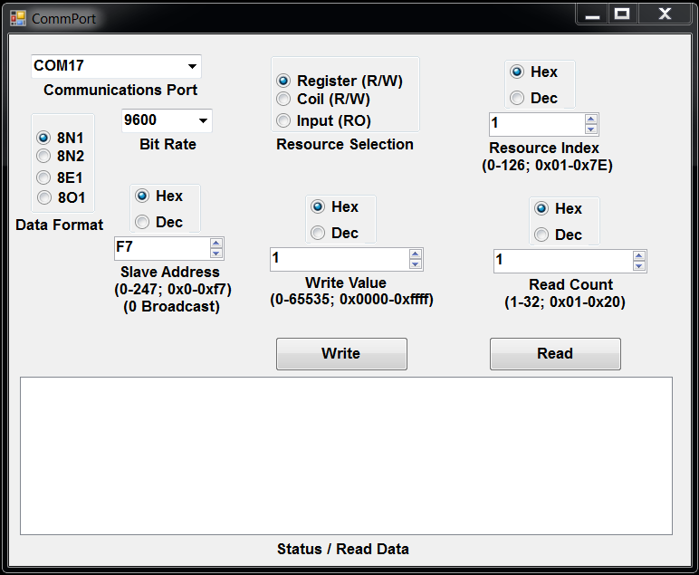
Modbus Windows register access program: ModbusDeviceAccess
These programs are used to perform accesses to the Modbus devices register set. It allows the writing of arbitrary hex data to any hex register address one at a time and the reading of blocks of arbitrary data from any hex register addres displayed in hex, signed, or unsigned decimal.
- Use of this utility requires the following steps:
- 1. Select the COM port from the drop down box
- 2. Select the bit rate from the drop down box
- 3. Select the correct data format (8N1 is default)
- 4. Enter the connected device slave address after selecting the format (Hex or Decimal)
- NOTICE:The coil functionality is currently not functional in Windows
- 5. Select the resource type (Regoster, Input, or Coil)
- 6a. Set the resoucw index (e.g., Register number) and count for reading
- 6b. Set the resoucw index (e.g., Register number) and value for writing
- 7. Click the appropriate button to read or write the device
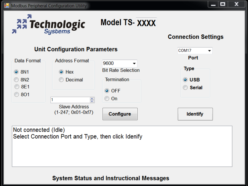
Modbus Windows device configuration program: ModbusDeviceConfigure
This program is used to perform configuration of a Technologic Systems Modbus device. On older Modbuc devices these settings (Slave address, Communications bit rate and data format, termination) would have been performed via DIP switches. This configuration information is stored in non-volatile memory on the device. This utility is designed to operate on devices confired as factory degault, 9600, N81, address 0cf7. Windows USB connections are not currently supported, so the devie should be connected via a TS-142 ISB to Serial Modbus adapter is required.
- Use of this utility requires the following steps:
- 1. Select the COM port from the drop down box
- NOTICE:The USB functionality is currently not operational on Windows
- 2. Select the COM port type (USB or Serial)
- 3. Click Identify
- The model willl appear at the top of the page
- 4. Select the Data Format, Slave Address, Bit Rate, and Termination
- 5. Click Configure
Modbus TS-1420 Management Utility
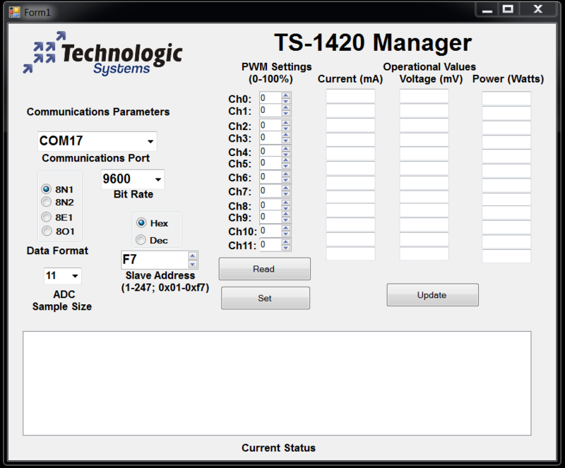
Modbus Windows program: TS1420Manager
These programs are used to operate the functionality of the TS-1420
- Use of this utility requires the following steps:
- 1. Select the COM port from the drop down box
- 2. Select the bit rate from the drop down box
- 3. Select the data format (8N1 is default)
- 4. Enter the connected device slave address after selecting the format (Hex or Decimal)
- 5. Select the proper ADC sample size
- 6. Select or set the desired [ercentage of PWM operation per channel
- 7a. Click the Set button to set the ADC and PWM values
- 7a. Alternately click the Read button to read the current values
- 8. Clicke the update button to display the per channel voltage and current and display the calculated power
FCC Advisory
This equipment generates, uses, and can radiate radio frequency energy and if not installed and used properly (that is, in strict accordance with the manufacturer's instructions), may cause interference to radio and television reception. It has been type tested and found to comply with the limits for a Class A digital device in accordance with the specifications in Part 15 of FCC Rules, which are designed to provide reasonable protection against such interference when operated in a commercial environment. Operation of this equipment in a residential area is likely to cause interference, in which case the owner will be required to correct the interference at his own expense.
If this equipment does cause interference, which can be determined by turning the unit on and off, the user is encouraged to try the following measures to correct the interference:
Reorient the receiving antenna. Relocate the unit with respect to the receiver. Plug the unit into a different outlet so that the unit and receiver are on different branch circuits. Ensure that mounting screws and connector attachment screws are tightly secured. Ensure that good quality, shielded, and grounded cables are used for all data communications. If necessary, the user should consult the dealer or an experienced radio/television technician for additional suggestions. The following booklets prepared by the Federal Communications Commission (FCC) may also prove helpful:
How to Identify and Resolve Radio-TV Interference Problems (Stock No. 004-000-000345-4) Interface Handbook (Stock No. 004-000-004505-7) These booklets may be purchased from the Superintendent of Documents, U.S. Government Printing Office, Washington, DC 20402.
Limited Warranty
See our Terms and Conditions for more details.


